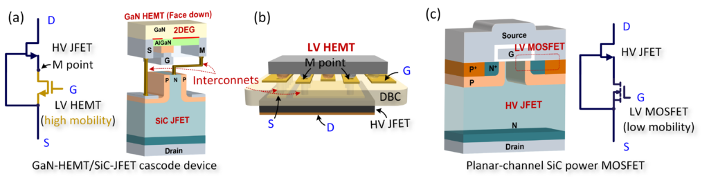
Introduction of HyFET Fig. 1 The configuration of the GaN/SiC HyFET. (b) The face-to-face 3D stacked GaN/SiC cascode device with minimized interconnect inductance. (c) The SiC MOSFET structure and the internal cascode configuration of a HV JFET and a LV MOSFET. Here is the HyFET structure ! Edit for example